
Introduction – Have scientists actually captured real pictures of atoms?
Have scientists actually captured real pictures of atoms, or are all those glowing spheres and electron clouds just diagrams? Most of us first learn about atoms through simple drawings, with circles for nuclei and rings for electrons. Those models help us understand basic concepts but they are not photographs. Thanks to instruments like the scanning tunneling microscope (STM) and the atomic force microscope (AFM), researchers can probe surfaces at the atomic scale and collect data that map out individual atoms. In this post we will explore how STM works, examine techniques such as AFM and transmission electron microscopy (TEM), and showcase genuine micrographs that reveal atoms in all their tiny, tactile detail.
When Did Scientists See Atoms for Real?
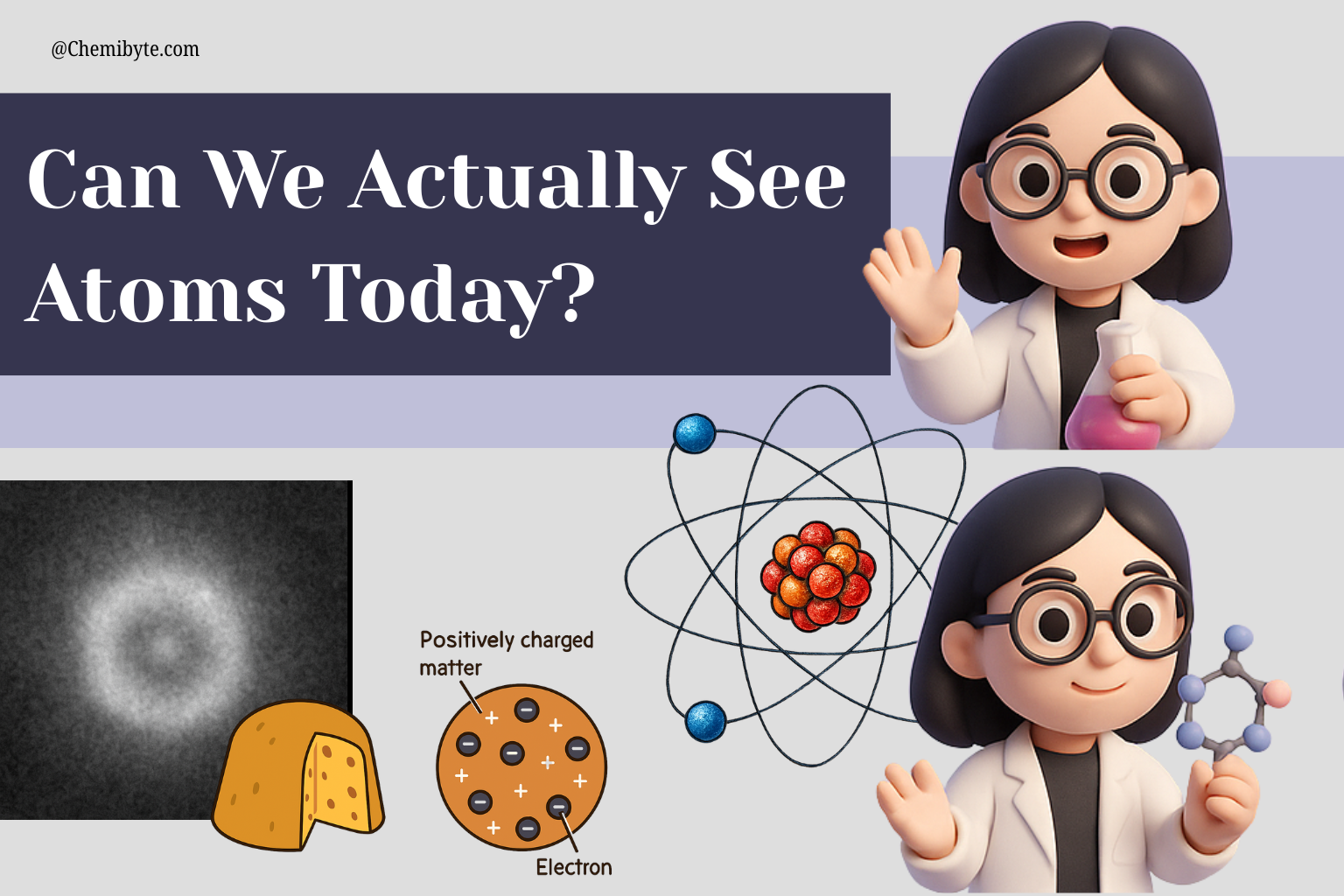
Scientists first imagined atoms more than two thousand years ago, and over time they refined their ideas and atomic models. In the early 1800s, John Dalton proposed that matter is made of indivisible particles called atoms. In 1904, J. J. Thomson introduced the plum-pudding model, picturing the atom as a diffuse sphere of positive charge with electrons embedded like plums in a pudding. In 1911, Ernest Rutherford’s gold-foil experiments revealed that nearly all of an atom’s mass and positive charge lies in a tiny central nucleus. He proposed that electrons must orbit this nucleus, much like planets orbit the Sun.
Building on Rutherford’s work, Niels Bohr in 1913 proposed that electrons move in fixed, quantized energy levels around the nucleus—a model that remains a useful approximation today.
Even with all these theoretical breakthroughs, no one had actually seen an atom.
That changed in the 20th century with the development of powerful new imaging tools. In 1937, Manfred von Ardenne built the first scanning electron microscope (SEM). Although SEM could not resolve individual atoms, it provided highly detailed views of surfaces down to a few nanometres—an important stepping stone.
Then, in 1981, a real breakthrough occurred. Gerd Binnig and Heinrich Rohrer invented the scanning tunneling microscope (STM). This instrument used a quantum tunneling current and a razor-sharp tip to scan conductive surfaces, producing the first real images of individual atoms.
What Did the First Real Images of Atoms Look Like?
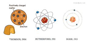
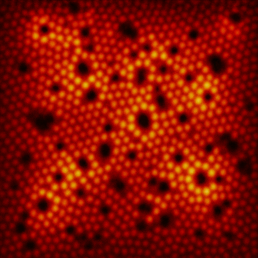
Imagine looking at a perfectly dark surface—and then, suddenly, you see tiny, glowing dots twinkling like stars in the night sky. That’s exactly what scientists saw the first time they imaged atoms using a powerful new tool called the scanning tunneling microscope (STM).
In 1982, researchers at IBM Zurich used STM to scan a clean piece of silicon. But this microscope didn’t use light like regular microscopes do. Instead, it used something far more unusual—a super-sharp metal tip that moved across the surface, getting so close that it was just a few atoms away.
As the tip moved, it measured a tiny electric current that could “jump” through the space between the tip and the atoms on the surface. This is called tunneling current, and it changes depending on how near the tip is to an atom.
By carefully measuring those changes, the STM built a detailed picture—like a map—of the surface at the atomic level. And in that picture, each glowing bump you see is a real, individual atom. For the first time in history, scientists weren’t just drawing or imagining atoms—they could actually see them.
From Atoms to Surfaces: How SEM Set the Stage
But before scientists had STM, they already had another amazing tool: the scanning electron microscope (SEM). SEM can’t see individual atoms, but it was the first machine that let scientists explore surfaces at a super small scale, way smaller than anything a regular microscope could handle.
You can think of it this way:
-
STM is like using a super-sensitive finger to “feel” the surface of atoms.
-
SEM is like using a flashlight made of electrons to look at tiny details on the surface of things.
SEM helped scientists study surfaces with incredible magnification and detail, from the ridges on a grain of sand to the grooves on a microchip. Even though it didn’t show atoms directly, SEM paved the way for atomic imaging by helping researchers explore the world at the nanoscale.
What Is Scanning Electron Microscopy (SEM) – and How Does It Work?
![]() Invented in 1937 by German physicist Manfred von Ardenne, SEM gave scientists their first close-up look at surfaces in the micro and nanometre range.
Invented in 1937 by German physicist Manfred von Ardenne, SEM gave scientists their first close-up look at surfaces in the micro and nanometre range.
![]() What Makes SEM Different?
What Makes SEM Different?
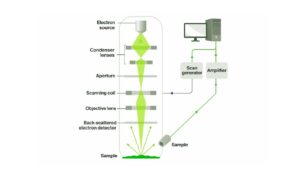
Instead of using light like a traditional microscope, SEM uses a beam of electrons. These electrons are fired at a sample and scan across its surface. As they hit the surface, they interact with the atoms and release signals that are used to build an image.
If a light microscope is like using your eyes, SEM is like using a flashlight made of electrons to explore a tiny world.
How SEM Works – Step by Step
- Preparing the Sample
The sample—like a piece of metal, plastic, or even an insect—is coated with a thin layer of a conductive material (like gold or carbon) and placed inside a vacuum. - Firing the Electron Beam
SEM uses an electron gun to shoot a stream of electrons, which are focused into a fine beam using electromagnetic lenses. - Scanning the Surface
The beam moves across the surface in a grid pattern. When electrons hit the sample, they bounce back or cause other signals to be emitted. - Collecting the Signals
SEM detects these signals:- Secondary electrons – create high-resolution surface images
- Backscattered electrons – help show contrast between materials
- X-rays – reveal what elements are present in the sample
- Forming the Image
A detector collects these signals and builds a detailed, black-and-white image on the computer screen—line by line.
Why SEM Was So Useful
- Incredible Magnification
SEM can magnify objects up to 1,000,000 times—much more than any light microscope. - Amazing Surface Detail
It shows very fine textures—cracks, edges, tiny holes, and surface shapes—perfect for studying materials, bugs, circuits, and more. - Element Identification
With a feature called EDS (Energy Dispersive X-ray Spectroscopy), SEM can even tell what elements are in a sample. - Wide Sample Variety
SEM works on metals, plastics, rocks, bugs, fabrics, electronics, and more.
What Does an SEM Image Look Like?
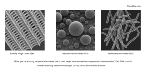
SEM images look like black-and-white photographs with extremely sharp details. You can clearly see:
- The tiny scales on a butterfly wing
- The grooves in a grain of sand
- Micro-cracks in a piece of metal
- The fine structure of a microchip
Why SEM Mattered in the History of Atom Imaging
Even though SEM can’t see individual atoms, it was a huge step forward. It allowed scientists to study structures far smaller than light could ever reveal—and it helped pave the way for atomic-level imaging with STM and AFM.
Next, let’s look at how Atomic Force Microscopy (AFM) gave us the power to “feel” individual atoms—even on non-conductive surfaces.
What Is Scanning Tunneling Microscopy (STM) – and How Does It Work?
The scanning tunneling microscope (STM), invented in 1981 by Gerd Binnig and Heinrich Rohrer, was the first instrument to capture real images of individual atoms. It works using a fascinating principle from quantum mechanics—tunneling.
How STM Works – Step by Step
1. A Sharp Metal Tip
STM uses an ultra-sharp metal tip, so fine that the end is just a few atoms wide.
2. Getting Close—Really Close
The tip is brought extremely close to a surface—less than a nanometre away. At this range, electrons can actually “tunnel” through the tiny gap between the tip and the surface.
3. Measuring the Tunneling Current
This tunneling produces a tiny electric current. The STM measures how this current changes as the tip moves across the surface.
4. Building an Atomic Map
By recording these changes, the microscope creates a super-detailed map of the surface. Each bump or dip in the map corresponds to the position of individual atoms.
What Makes STM So Powerful?
-
Atomic Resolution: STM was the first tool ever to “see” atoms directly.
-
Works on Conductive Surfaces: It requires the surface to conduct electricity, so it’s mostly used with metals or semiconductors.
-
Paved the Way for Nanotechnology: STM didn’t just reveal atoms—it eventually let scientists move them.
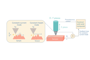
What Is Atomic Force Microscopy (AFM) – and How Does It Work?
After the success of the STM, scientists realized they needed a similar tool that could work on more types of materials—not just metals. That’s where Atomic Force Microscopy (AFM) came in. It was developed in 1986 by Gerd Binnig (who also co-invented STM), along with Calvin Quate and Christoph Gerber.
How Is AFM Different from STM?
While STM uses electric current to measure atoms (so it only works on conductive surfaces), AFM uses physical touch. Think of it like this:
If STM is like “seeing” with electricity, then AFM is like “feeling” with your fingertips.
How AFM Works – Step by Step
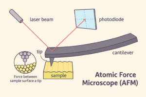
- The Tiny Tip and Cantilever
AFM has an extremely sharp tip—so sharp that the end is just a few atoms wide. This tip is attached to a thin, flexible arm called a cantilever (like a diving board on the nanoscale). - Touching the Surface
As the tip moves across the surface of the material, it gets extremely close to the atoms—so close that tiny atomic forces (like attraction or repulsion) start to act between the tip and the surface. - Measuring the Forces
These forces make the cantilever bend slightly—up and down—depending on the texture of the surface. A laser beam shines on the back of the cantilever and reflects into a detector. The movement of the laser tells the computer exactly how much the cantilever is bending. - Creating the Image
As the tip scans across the entire surface, the microscope records all those little bends and movements. The result is a detailed 3D map of the surface—showing bumps, valleys, and even individual atoms in some cases.
What Makes AFM So Special?
- Works on Almost Any Material
Unlike STM, AFM can scan non-conductive materials like:- Plastics and polymers
- Ceramics
- Glass
- Biological samples (cells, DNA, proteins)
- High Resolution
AFM can detect features smaller than a nanometre—sometimes even individual atoms or molecules. - No Special Conditions Needed
AFM doesn’t need a vacuum or extreme cooling. It can work in air, in liquids, or even inside living cells, which makes it perfect for biological and medical research.
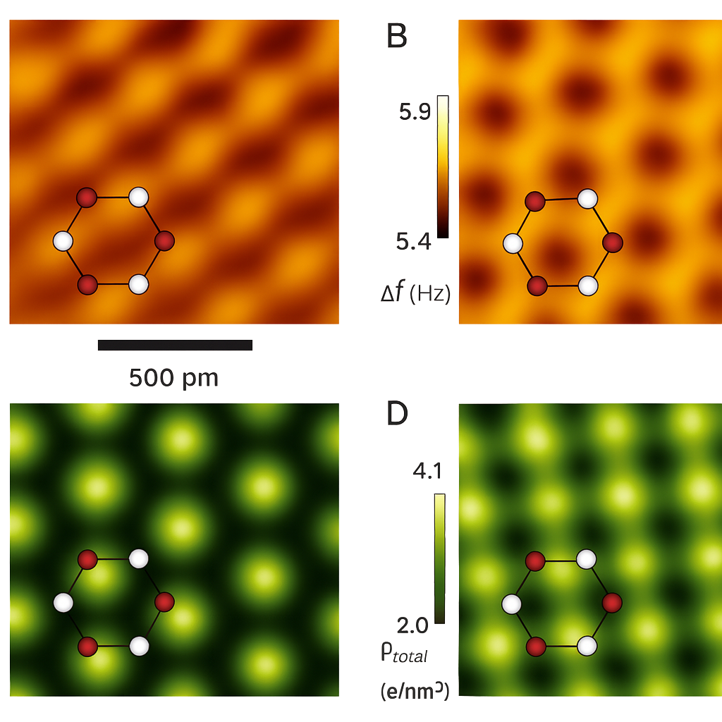
What Does an AFM Image Look Like?
AFM images usually appear as 3D maps of surfaces. You can clearly see textures, ridges, grooves, and sometimes rows of atoms. For example:
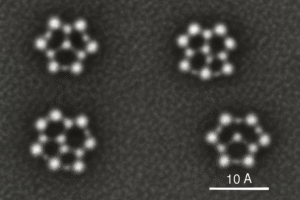
- A strand of DNA might look like a twisting rope.
- A cell surface might show soft, bumpy terrain.
- A nanomaterial might reveal repeating atomic patterns.
In short, AFM gave scientists a new set of eyes—ones that could “feel” almost any surface with atomic-level precision. It expanded atomic imaging far beyond metals and gave researchers access to the tiniest details of everyday materials, molecules, and even life itself.
Transmission Electron Microscopy (TEM)
At the same time, TEM was improved to the point where it could also reveal atoms. Instead of a tip, TEM shoots a beam of electrons through an ultra-thin sample. Atoms in the sample block or bend the beam, forming an image that shows columns of atoms as tiny dots. This helped scientists see the inside of materials at the atomic level.
From Seeing to Controlling
Once we could see atoms, researchers started to move them. Using STM or AFM tips, scientists carefully nudged atoms across a surface—spelling out letters, making tiny patterns, and proving that we could not only observe atoms, but control them one by one.
The Rise of Nanotechnology
This control launched the field of nanotechnology. Engineers began designing materials and devices atom by atom—building faster computers, sensors, and even early components for quantum machines.
Trapping Single Atoms with Light
In recent years, scientists have learned to trap single atoms using lasers and optical tweezers. These techniques let researchers hold an atom in place and watch it glow, helping build atomic clocks and explore quantum physics.
In Summary
In just a few decades, science moved from wondering if atoms were real to seeing them, moving them, and engineering with them. What once seemed invisible and untouchable became something we could study—and even build with—one atom at a time.
What Came After AFM?
Once scientists could “feel” atoms with AFM, they continued pushing the limits of resolution and imaging methods. That led to another powerful tool:
What Is Transmission Electron Microscopy (TEM)?
Transmission Electron Microscopy (TEM) takes a different approach from STM or AFM. Instead of scanning the surface, it shoots a beam of electrons through a sample that is incredibly thin—just a few nanometres thick.
How TEM Works – Step by Step
-
Ultra-Thin Sample
The sample is sliced so thin that electrons can pass through it. -
Electron Beam
A beam of electrons is fired at the sample. As it passes through, the beam interacts with the atoms inside. -
Image Formation
Electrons that pass through (or are scattered) hit a detector or screen, creating an image based on atomic structure. -
Extreme Detail
The resulting image can show rows or columns of atoms in crystals, defects, grain boundaries, and even the shape of nanomaterials.
What Makes TEM Powerful?
-
Can view inside a sample, not just the surface
-
Reveals atomic structure and arrangement
-
Ideal for studying materials science, nanotechnology, and semiconductors
-
Modern TEMs can even film atomic movement in real time
What Is Optical Trapping of Single Atoms?

More recently, scientists developed ways to hold single atoms in mid-air using light. This technique is called optical trapping, often used in quantum physics experiments.
How Optical Trapping of single atom Works:
-
Laser Cooling slows atoms down until they’re nearly still
-
Optical Tweezers (focused laser beams) hold one atom in place
-
Detectors measure the atom’s glow (fluorescence), letting researchers track its behavior
This method is used in building atomic clocks, studying quantum properties, and testing fundamental physics.
Conclusion: From Models to Reality
For most of history, atoms were just an idea—imagined, theorized, and drawn in diagrams. But today, with tools like STM, AFM, SEM, TEM, and optical traps, scientists can not only see atoms… they can move them, measure them, and build with them.
Real images of atoms changed everything. They turned theory into reality and launched a new era of nanoscience, quantum research, and atomic-level engineering.
Are Real Atom Photos the Same as Diagrams in Books?
Not exactly. The real photos of atoms—captured using tools like STM, AFM, or TEM—look very different from the neat, colorful diagrams we see in textbooks.
Here’s why:
-
Real images are based on data, not color or shape
These microscopes don’t use light. Instead, they detect forces, electrical signals, or electron scattering. The result is a pattern of bright spots, shadows, or bumps—often shown in grayscale or computer-generated color. -
Textbook diagrams are simplified for learning
In books, atoms are shown as perfect circles with clearly drawn shells and orbits. That helps us understand structure, but it doesn’t reflect what atoms truly look like under a microscope. -
Real atom photos show surfaces, not full structure
STM and AFM, for example, only show the top layer of atoms—what’s exposed on a surface. You won’t see the nucleus or electron orbits like you would in a Bohr diagram.
Absolutely! Here’s that section revised and expanded for clarity, keeping your structure and adding a strong heading optimized for SEO:
What Have Scientists Learned from Imaging Atoms?
The ability to capture real images of atoms has completely changed how scientists understand and work with matter at the smallest scale. These advanced imaging techniques—like STM, AFM, SEM, and TEM—have led to major breakthroughs across multiple fields.
Here’s what scientists have gained from being able to see atoms:
- Confirmed the Structure of Elements and Molecules
Real images have validated theoretical models of atomic and molecular arrangements, helping chemists and physicists prove what was once only predicted. - Observed How Atoms Move, Bond, and React
Using advanced time-lapse microscopy, researchers can now watch atoms shift during chemical reactions, bond formation, or material transformations. - Designed Stronger, Smarter Materials
Atomic imaging has allowed engineers to build materials one atom at a time—creating ultra-thin films, nanodevices, and smart surfaces with precise properties. - Launched Entire New Fields
Fields like nanotechnology, quantum computing, and precision medicine rely heavily on atomic-level control. These technologies wouldn’t exist without real imaging.
Today, seeing atoms is not just about curiosity—it’s about building the future, one atom at a time.
Key Takeaways
Let’s wrap up everything you’ve learned in this blog:
-
Scientists imagined atoms long before they could see them—starting with theories from Dalton, Thomson, Rutherford, and Bohr.
-
The first real image of atoms was captured in 1982 using the scanning tunneling microscope (STM).
-
Tools like AFM, SEM, TEM, and optical trapping now let scientists study, touch, and even move individual atoms.
-
Real atom images don’t look like diagrams—they show measured data, not perfect circles or orbits.
-
These tools helped launch major advancements in nanotechnology, material design, and quantum science.
Glossary
| Term | Simple Definition |
|---|---|
| Atom | The smallest unit of matter, made of protons, neutrons, and electrons. |
| STM (Scanning Tunneling Microscope) | A microscope that uses electric current to map individual atoms on conductive surfaces. |
| AFM (Atomic Force Microscope) | A microscope that “feels” atoms using a tiny flexible tip, ideal for both conductive and non-conductive materials. |
| SEM (Scanning Electron Microscope) | Uses an electron beam to scan and create detailed images of a surface, down to the nanoscale. |
| TEM (Transmission Electron Microscope) | Sends electrons through an ultra-thin sample to reveal the internal arrangement of atoms. |
| Optical Trapping | A technique that uses lasers to hold and observe individual atoms in place. |
| Tunneling Current | A very small electric current that flows when a tip comes extremely close to a surface, used in STM to detect atomic positions. |
| Cantilever | A flexible lever used in AFM that bends in response to atomic forces, creating a map of the surface. |
| Electron Beam | A stream of electrons used in SEM and TEM to interact with the sample and generate images. |
| Fluorescence | Light emitted by atoms when excited by a laser, often used to detect single atoms in optical traps. |
what surprised you the most?
Was it the idea that we can move atoms one by one? Or that some microscopes “feel” atoms instead of seeing them?
Drop your thoughts in the comments!
We’d love to hear what amazed you, confused you, or made you see science in a new way.
Have a question about atomic microscopes or want to request a new topic?
Ask below or contact us—we’d love to help you understand the invisible world, one atom at a time.
About the Author
Written by RK Aera
I’m the creator of Chemibyte, a calm and simple chemistry blog built for students, self-learners, and curious minds around the world. With a BSc in Chemistry and an MSc in Chemistry, I combine academic expertise with a passion for clear, visual science education.
I write every post to help you understand complex topics step by step—without the overwhelm. Whether you’re revising for your GCSEs, prepping for university exams, or just curious about how atoms really look, Chemibyte is your safe space to learn science with clarity and confidence.
Further readings
Worth reading!
thank you